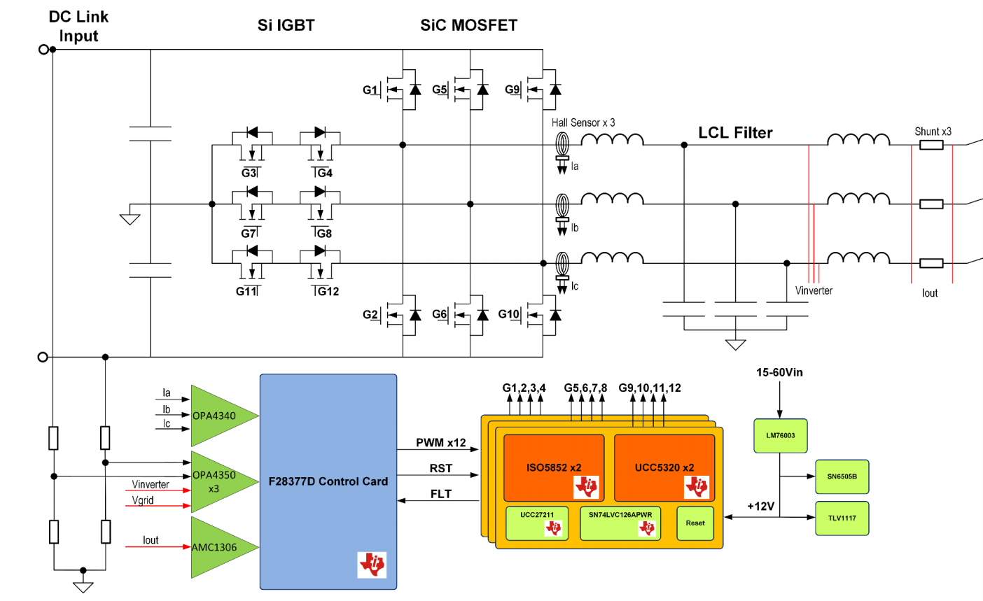
10kW 双向三相三级sic CAR CHARGER参考设计
这一经过验证的参考设计概述了如何实现基于 SiC 的三级三相直流/交流 T 型逆变器级。50KHz 的较高开关频率减小了滤波器设计的磁性元件尺寸,并因此提高了功率密度。通过使用可降低开关损耗的 SiC MOSFET,可确保实现高达 1000V 的更高直流总线电压和更低的开关损耗,从而达到 99% 的峰值效率。此设计可配置为两级或三级逆变器。该系统由单个 C2000 微控制器 (MCU) TMS320F28379D 进行控制,可在所有运行模式下为所有电源电子开关器件生成 PWM 波形。
特性
- 额定标称输入电压/最大输入电压:800V/1000VDC
- 在 400VAC 50/60Hz T 型连接时的最大输出功率为 10kW/10KVA
- 工作时的功率因数范围为 0.7 滞后至 0.7 超前
- 基于高压 (1200V) SiCMosFET 的全桥逆变器,峰值效率高达 99%
- 满载时的输出电流 THD 小于 2%
- 使用 AMC1301 进行隔离式电流检测,从而实现负载电流监测
用于驱动高压 SiC MOSFET 并具有增强型隔离功能的隔离式驱动器 ISO5852S,以及用于驱动中间 Si IGBT 的 UCC5320S
2 System Overview 2.1 Block Diagram Figure 2-1. TIDA-01606 Block Diagram This reference design is comprised of four separate boards that intercommunicate. The following boards work in tandem to form this three-phase inverter reference design: • A power board, comprising all of the switching device, LCL filter, sensing electronics, and power structure • A TMS320F28379D Control Card to support the DSP • Three gate driver cards, each with two ISO5852S and two UCC5320 gate drivers • A DC bus voltage measuring board (TIDA-01606 ISOHVCARD)

2.2 Highlighted Products 2.2.1 ISO5852S The ISO5852S device is a 5.7-kVRMS, reinforced isolated gate driver for IGBTs and MOSFETs with split outputs, OUTH and OUTL, providing 2.5-A source and 5-A sink current. The input side operates from a single 2.25-V to 5.5-V supply. The output side allows for a supply range from minimum 15 V to maximum 30 V. Two complementary CMOS inputs control the output state of the gate driver. The short propagation time of 76 ns provides accurate control of the output stage. • 100-kV/μs minimum common-mode transient immunity (CMTI) at VCM = 1500 V • Split outputs to provide 2.5-A peak source and 5-A peak sink currents • Short propagation delay: 76 ns (typ), 110 ns (max) • 2-A active Miller clamp • Output short-circuit clamp • Soft turnoff (STO) during short circuit • Fault alarm upon desaturation detection is signaled on FLT and reset through RST • Input and output undervoltage lockout (UVLO) with Ready (RDY) pin indication • Active output pulldown and default low outputs with low supply or floating inputs • 2.25-V to 5.5-V input supply voltage • 15-V to 30-V output driver supply voltage www.ti.com System Overview TIDUE53G – MARCH 2018 – REVISED SEPTEMBER 2022 Submit Document Feedback 10-kW, Bidirectional Three-Phase Three-Level (T-type) Inverter and PFC Reference Design 3 Copyright © 2022 Texas Instruments Incorporated• CMOS compatible inputs • Rejects input pulses and noise transients shorter than 20 ns • Operating temperature: –40°C to +125°C ambient • Isolation surge withstand voltage of 12800-VPK GND1 VEE2 RST RDY FLT IN+ IN± VCC1 VCC2 DESAT GND2 OUTH OUTL CLAMP VCC1 VCC1 UVLO1 Mute Decoder Q SR Q VCC1 VCC1 Gate Drive and Encoder Logic UVLO2 2 V 9 V 500 µA STO VCC2 Ready Fault Figure 2-2. ISO5852S Functional Block Diagram 2.2.2 UCC5320 The UCC53x0 is a family of compact, single-channel, isolated IGBT, SiC, and MOSFET gate drivers with superior isolation ratings and variants for pinout configuration, and drive strength. The UCC53x0 is available in an 8-pin SOIC (D) package. This package has a creepage and clearance of 4 mm and can support isolation voltage up to 3 kVRMS, which is good for applications where basic isolation is needed. With these various options and wide power range, the UCC53x0 family is a good fit for motor drives and industrial power supplies. • 3-V to 15-V input supply voltage • 13.2-V to 33-V output driver supply voltage • Feature options: – Split outputs (UCC5320S and UCC5390S) – UVLO with respect to IGBT emitter (UCC5320E and UCC5390E) – Miller clamp option (UCC5310M and UCC5350M) • Negative 5-V handling capability on input pins • 60-ns (typical) propagation delay for UCC5320S, UCC5320E, and UCC5310M • 100-kV/µs minimum CMTI • Isolation surge withstand voltage: 4242 VPK • Safety-related certifications: – 4242-VPK isolation per DIN V VDE V 0884-10 and DIN EN 61010-1 (planned) – 3000-VRMS isolation for 1 minute per UL 1577 (planned) – CSA Component Acceptance Notice 5A, IEC 60950-1 and IEC 61010-1 End Equipment Standards (Planned) – CQC Certification per GB4943.1-2011 (Planned) System Overview www.ti.com 4 10-kW, Bidirectional Three-Phase Three-Level (T-type) Inverter and PFC Reference Design TIDUE53G – MARCH 2018 – REVISED SEPTEMBER 2022 Submit Document Feedback Copyright © 2022 Texas Instruments Incorporated• 4-kV ESD on all pins • CMOS inputs • 8-pin narrow body SOIC package • Operating temperature: –40°C to +125°C ambient text VCC2 UVLO, Level Shift and Control Logic VCC2 VOUTH IN± IN+ VOUTL VCC1 VEE2 GND1 UVLO and Input Logic 15 V Rest of Circuit 5 V Figure 2-3. UCC5320 Functional Block Diagram (S Version) 2.2.3 TMS320F28379D The Delfino™ TMS320F2837xD is a powerful 32-bit floating-point microcontroller unit (MCU) designed for advanced closed-loop control applications such as industrial drives and servo motor control; solar inverters and converters; digital power; transportation; and power line communications. Complete development packages for digital power and industrial drives are available as part of the powerSUITE and DesignDRIVE initiatives. While the Delfino product line is not new to the TMS320C2000™ portfolio, the F2837xD supports a new dual-core C28x architecture that significantly boosts system performance. The integrated analog and control peripherals also let designers consolidate control architectures and eliminate multiprocessor use in high-end systems. • Dual-core architecture: – Two TMS320C28x 32-bit CPUs – 200 MHz – IEEE 754 single-precision floating-point unit (FPU) – Trigonometric math unit (TMU) – Viterbi/complex math unit (VCU-II) • Two programmable control law accelerators (CLAs) – 200 MHz – IEEE 754 single-precision floating-point instructions – Executes code independently of main CPU • On-chip memory – 512KB (256 kW) or 1MB (512 kW) of Flash (ECC-protected) – 172KB (86 kW) or 204KB (102 kW) of RAM (ECC-protected or parity-protected) – Dual-zone security supporting third-party development • Clock and system control: – Two internal zero-pin 10-MHz oscillators – On-chip crystal oscillator – Windowed watchdog timer module – Missing clock detection circuitry • 1.2-V core, 3.3-V I/O design • System peripherals: – Two external memory interfaces (EMIFs) with ASRAM and SDRAM support – Dual six-channel direct memory access (DMA) controllers

