0755-28286748
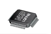
16-bit MCU, S12X core, 1MB Flash, 50MHz, -40/+125degC, Automotive Qualified,
The MC9S12XE-Family of micro controllers is a further development of the S12XD-Family including new features for enhanced system integrity and greater functionality. These new features include a Memory Protection Unit (MPU) and Error Correction Code (ECC) on the Flash memory together with enhanced EEPROM functionality (EEE), an enhanced XGATE, an Internally filtered, frequency modulated Phase Locked Loop (IPLL) and an enhanced ATD. The E-Family extends the S12X product range up to 1MB of Flash memory with increased I/O capability in the 208-pin version of the flagship MC9S12XE100. The MC9S12XE-Family delivers 32-bit performance with all the advantages and efficiencies of a 16 bit MCU. It retains the low cost, power consumption, EMC and code-size efficiency advantages currently enjoyed by users of Freescale’s existing 16-Bit MC9S12 and S12X MCU families. There is a high level of compatibility between the S12XE and S12XD families. The MC9S12XE-Family features an enhanced version of the performance-boosting XGATE co-processor which is programmable in “C” language and runs at twice the bus frequency of the S12X with an instruction set optimized for data movement, logic and bit manipulation instructions and which can service any peripheral module on the device. The new enhanced version has improved interrupt handling capability and is fully compatible with the existing XGATE module. The MC9S12XE-Family is composed of standard on-chip peripherals including up to 64Kbytes of RAM, eight asynchronous serial communications interfaces (SCI), three serial peripheral interfaces (SPI), an 8- channel IC/OC enhanced capture timer (ECT), two 16-channel, 12-bit analog-to-digital converters, an 8- channel pulse-width modulator (PWM), five CAN 2.0 A, B software compatible modules (MSCAN12), two inter-IC bus blocks (IIC), an 8-channel 24-bit periodic interrupt timer (PIT) and an 8-channel 16-bit standard timer module (TIM). The MC9S12XE-Family uses 16-bit wide accesses without wait states for all peripherals and memories. The non-multiplexed expanded bus interface available on the 144/208-Pin versions allows an easy interface to external memories. In addition to the I/O ports available in each module, up to 26 further I/O ports are available with interrupt capability allowing Wake-Up from STOP or WAIT modes. The MC9S12XE-Family is available in 208- Pin MAPBGA, 144-Pin LQFP, 112-Pin LQFP or 80-Pin QFP options. 1.1.1 Features Features of the MC9S12XE-Family are listed here. Please see Table D-2.for memory options and Table D2. for the peripheral features that are available on the different family members. Chapter 1 Device Overview MC9S12XE-Family MC9S12XE-Family Reference Manual Rev. 1.25 28 Freescale Semiconductor • 16-Bit CPU12X — Upward compatible with MC9S12 instruction set with the exception of five Fuzzy instructions (MEM, WAV, WAVR, REV, REVW) which have been removed — Enhanced indexed addressing — Access to large data segments independent of PPAGE • INT (interrupt module) — Eight levels of nested interrupts — Flexible assignment of interrupt sources to each interrupt level. — External non-maskable high priority interrupt (XIRQ) — Internal non-maskable high priority Memory Protection Unit interrupt — Up to 24 pins on ports J, H and P configurable as rising or falling edge sensitive interrupts • EBI (external bus interface)(available in 208-Pin and 144-Pin packages only) — Up to four chip select outputs to select 16K, 1M, 2M and up to 4MByte address spaces — Each chip select output can be configured to complete transaction on either the time-out of one of the two wait state generators or the deassertion of EWAIT signal • MMC (module mapping control) • DBG (debug module) — Monitoring of CPU and/or XGATE busses with tag-type or force-type breakpoint requests — 64 x 64-bit circular trace buffer captures change-of-flow or memory access information • BDM (background debug mode) • MPU (memory protection unit) — 8 address regions definable per active program task — Address range granularity as low as 8-bytes — No write / No execute Protection Attributes — Non-maskable interrupt on access violation • XGATE — Programmable, high performance I/O coprocessor module — Transfers data to or from all peripherals and RAM without CPU intervention or CPU wait states — Performs logical, shifts, arithmetic, and bit operations on data — Can interrupt the HCS12X CPU signalling transfer completion — Triggers from any hardware module as well as from the CPU possible — Two interrupt levels to service high priority tasks — Hardware support for stack pointer initialisation • OSC_LCP (oscillator) — Low power loop control Pierce oscillator utilizing a 4MHz to 16MHz crystal — Good noise immunity — Full-swing Pierce option utilizing a 2MHz to 40MHz crystal — Transconductance sized for optimum start-up margin for typical crystals • IPLL (Internally filtered, frequency modulated phase-locked-loop clock generation
CAR
| 型号 | DataSheet | Dimension (mm) | Description |
|---|

 主芯片和MCU
 模拟和接口芯片
 MEMS传感器
 网通WIFI芯片