0755-28286748
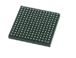
FPGA - 现场可编程门阵列 Lattice ECP5-5G; 83.6K LUTs; 1.2V; 5G SERDES
Each ECP5/ECP5-5G device contains an array of logic blocks surrounded by Programmable I/O Cells (PIC). Interspersed between the rows of logic blocks are rows of sysMEM™ Embedded Block RAM (EBR) and rows of sysDSP™ Digital Signal Processing slices, as shown in Figure 2.1. The LFE5-85 devices have three rows of DSP slices, the LFE5-45 devices have two rows, and both LFE5-25 and LFE5-12 devices have one. In addition, the LFE5UM/LFE5UM5G devices contain SERDES Duals on the bottom of the device. The Programmable Functional Unit (PFU) contains the building blocks for logic, arithmetic, RAM, and ROM functions. The PFU block is optimized for flexibility, allowing complex designs to be implemented quickly and efficiently. Logic Blocks are arranged in a two-dimensional array. The ECP5/ECP5-5G devices contain one or more rows of sysMEM EBR blocks. sysMEM EBRs are large, dedicated 18 Kb fast memory blocks. Each sysMEM block can be configured in a variety of depths and widths as RAM or ROM. In addition, ECP5/ECP5-5G devices contain up to three rows of DSP slices. Each DSP slice has multipliers and adder/accumulators, which are the building blocks for complex signal processing capabilities. The ECP5 devices feature up to four embedded 3.2 Gb/s SERDES channels, and the ECP5-5G devices feature up to four embedded 5 Gb/s SERDES channels. Each SERDES channel contains independent 8b/10b encoding / decoding, polarity adjust and elastic buffer logic. Each group of two SERDES channels, along with its Physical Coding Sublayer (PCS) block, creates a dual DCU (Dual Channel Unit). The functionality of the SERDES/PCS duals can be controlled by SRAM cell settings during device configuration or by registers that are addressable during device operation. The registers in every dual can be programmed via the SERDES Client Interface (SCI). These DCUs (up to two) are located at the bottom of the devices. Each PIC block encompasses two PIOs (PIO pairs) with their respective sysI/O buffers. The sysI/O buffers of the ECP5/ECP5-5G devices are arranged in seven banks (eight banks for LFE5-85 devices in caBGA756 and caBGA554 packages), allowing the implementation of a wide variety of I/O standards. One of these banks (Bank 8) is shared with the programming interfaces. Half of the PIO pairs on the left and right edges of the device can be configured as LVDS transmit pairs, and all pairs on left and right can be configured as LVDS receive pairs. The PIC logic in the left and right banks also includes pre-engineered support to aid in the implementation of high speed source synchronous standards such as XGMII, 7:1 LVDS, along with memory interfaces including DDR3 and LPDDR3. The ECP5/ECP5-5G registers in PFU and sysI/O can be configured to be SET or RESET. After power up and the device is configured, it enters into user mode with these registers SET/RESET according to the configuration setting, allowing the device entering to a known state for predictable system function. Other blocks provided include PLLs, DLLs and configuration functions. The ECP5/ECP5-5G architecture provides up to four Delay-Locked Loops (DLLs) and up to four Phase-Locked Loops (PLLs). The PLL and DLL blocks are located at the corners of each device. The configuration block that supports features such as configuration bit-stream decryption, transparent updates and dual-boot support is located at the bottom of each device, to the left of the SERDES blocks. Every device in the ECP5/ECP5-5G family supports a sysCONFIG™ ports located in that same corner, powered by VCCIO8, allowing for serial or parallel device configuration. In addition, every device in the family has a JTAG port. This family also provides an on-chip oscillator and soft error
• Consumer Electronics • Compute and Storage • Wireless Communications • Industrial Control Systems • Automotive System
| 型号 | DataSheet | Dimension (mm) | Description |
|---|

 主芯片和MCU
 模拟和接口芯片
 MEMS传感器
 网通WIFI芯片