0755-28286748
CrossLink-NX device contains an array of logic blocks surrounded by Programmable I/O Cells (PIC). Interspersed between the rows of logic blocks are rows of sysMEM Embedded Block RAM (EBR) and rows of sysDSP Digital Signal Processing blocks
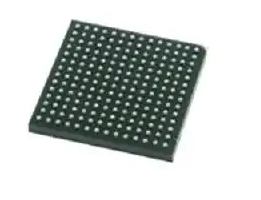
LIFCL-40-7MG121I Overview Each CrossLink-NX device contains an array of logic blocks surrounded by Programmable I/O Cells (PIC). Interspersed between the rows of logic blocks are rows of sysMEM Embedded Block RAM (EBR) and rows of sysDSP Digital Signal Processing blocks, as shown in Figure 2.1. The CrossLink-NX-40 devices have two rows of DSP blocks and contain three rows of sysMEM EBR blocks. In addition, CrossLink-NX-40 devices includes two Large SRAM blocks. The sysMEM EBR blocks are large, dedicated 18 Kb fast memory blocks and have built-in ECC and FIFO support. Each sysMEM block can be configured to a single, pseudo dual or true dual port memory in a variety of depths and widths as RAM or ROM. Each DSP block supports variety of multiplier, adder configurations with one 108-bit or two 54-bit accumulators supported, which are the building blocks for complex signal processing capabilities. Each PIC block encompasses two PIOs (PIO pairs) with their respective sysI/O buffers. The sysI/O buffers of the CrossLink-NX devices are arranged in seven banks allowing the implementation of a wide variety of I/O standards. The Wide Range (WR) I/O banks that are located in the top, left and right sides of the device provide flexible ranges of general purpose I/O configurations up to 3.3 V VCCIOs. The banks located in the bottom side of the device are dedicated to High Performance (HP) interfaces such as LVDS, MIPI, DDR3, LPDDR2, and LPDDR3 supporting up to 1.8 V VCCIOs. The Programmable Functional Unit (PFU) contains the building blocks for logic, arithmetic, RAM and ROM functions. The PFU block is optimized for flexibility, allowing complex designs to be implemented quickly and efficiently. Logic Blocks are arranged in a two-dimensional array. The registers in PFU and sysI/O blocks in CrossLink-NX devices can be configured to be SET or RESET. After power up and the device is configured, it enters into user mode with these registers SET/RESET according to the configuration setting, allowing the device entering to a known state for predictable system function. In addition, CrossLink-NX-40 devices provide various system level hard IP functional and interface blocks such as PCIe, D-PHY, I2C, SGMII/CDR, and ADC blocks. PCIe hard IP supports PCIe 2.0 and D-PHY supports up to 2.5 Gbps per lane. CrossLink-NX devices also provide security features to help secure user designs and deliver more robust reliability features to the user designs by using enhanced frame-based SED/SEC functions. Other blocks provided include PLLs, DLLs, and configuration functions. The PLL and DLL blocks are located at the corners of each device. CrossLink-NX devices also include Lattice Memory Mapped Interface (LMMI) which is a Lattice standardized interface for simple read and write operations to support controlling internal IPs. CrossLink-NX-40 devices has a dedicated ALUREG block to provide an ALU function to the RISC-V 32-bit processor and register file function. Every device in the family has a JTAG port. This family also provides an on-chip oscillator and soft error detect capability. The CrossLink-NX devices use 1.0 V as their core voltage
车载自动化,智能设备, 边缘计算,视频人脸识别
| 型号 | DataSheet | Dimension (mm) | Description |
|---|

 主芯片和MCU
 模拟和接口芯片
 MEMS传感器
 网通WIFI芯片