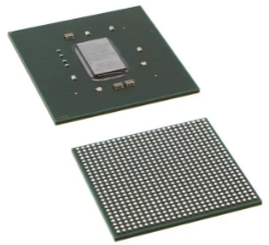
产品特性
XCKU115 提供最佳成本/性能/功耗比,包括在中端器件、下一代收发器和低成本封装中的最高信号处理带宽,实现性能与成本效益的最佳组合。此系列适合 100G 网络和数据中心应用的包处理,以及下一代医疗成像、 8k4k 视频和异构无线基础设施所需的 DSP 密集型处理。
特性
可编程系统集成
·多达 1.5M 系统逻辑单元,采用第 2 代 3D IC
·多芯片集成面向DSP 密集型应用
·多个集成式 PCI Express® Gen3 核
提升的系统性能
·8.2 TeraMAC DSP 计算性能
·高利用率使速度提升两个等级
·每个器件拥有高达 64 个 16G 支持背板的收发器。
·2,400Mb/s DDR4 可稳定工作在不同 PVT 条件下
BOM 成本削减
·系统集成降低应用 BOM 成本达 60%
·最慢速度极中的 12.5 Gb/s 收发器
·中间档速率等级芯片可支持 2,400 Mb/s DDR4
·VCXO 集成可降低时钟组件成本
总功耗削减
·较之上一代,达 40% 功耗降低
·通过 UltraScale 器件的类似于 ASIC 的时钟实现精细粒度时钟门控功能
·增强型系统逻辑单元封装减小动态功耗
加速设计生产力
·与 Virtex® UltraScale 器件引脚兼容,可扩展性高
·与 Vivado® Design Suite 协同优化,加快设计收敛
The Xilinx® Kintex® UltraScale™ FPGAs are available in -3, -2, -1, and -1L speed grades, with -3 having the
highest performance. The -1L devices can operate at either of two VCCINT voltages, 0.95V and 0.90V and
are screened for lower maximum static power. When operated at VCCINT = 0.95V, the speed specification
of a -1L device is the same as the -1 speed grade. When operated at VCCINT = 0.90V, the -1L performance
and static and dynamic power is reduced.
DC and AC characteristics are specified in commercial, extended, industrial, and military temperature
ranges. Except the operating temperature range or unless otherwise noted, all the DC and AC electrical
parameters are the same for a particular speed grade (that is, the timing characteristics of a -1 speed
grade industrial device are the same as for a -1 speed grade commercial device). However, only selected
speed grades and/or devices are available in each temperature range.
All supply voltage and junction temperature specifications are representative of worst-case conditions.
The parameters included are common to popular designs and typical applications.
This data sheet, part of an overall set of documentation on the UltraScale architecture-based devices, is
available on the Xilinx website at www.xilinx.com/documentation.
DC Characteristics
Kintex UltraScale FPGAs Data Sheet:
DC and AC Switching Characteristics
DS892 (v1.19) September 22, 2020 Product Specification
Table 1: Absolute Maximum Ratings(1)
Symbol Description Min Max Units
FPGA Logic
VCCINT Internal supply voltage –0.500 1.100 V
VCCINT_IO(2) Internal supply voltage for the I/O banks –0.500 1.100 V
VCCAUX Auxiliary supply voltage –0.500 2.000 V
VCCBRAM Supply voltage for the block RAM memories –0.500 1.100 V
VCCO
Output drivers supply voltage for HR I/O banks –0.500 3.400 V
Output drivers supply voltage for HP I/O banks –0.500 2.000 V
VCCAUX_IO(3) Auxiliary supply voltage for the I/O banks –0.500 2.000 V
VREF Input reference voltage –0.500 2.000 V
VIN(4)(5)(6)
I/O input voltage for HR I/O banks –0.400 VCCO + 0.550 V
I/O input voltage for HP I/O banks –0.550 VCCO + 0.550 V
I/O input voltage (when VCCO = 3.3V) for VREF and differential I/O
standards except TMDS_33(7) –0.400 2.625 V
Send Feedback
Kintex UltraScale FPGAs Data Sheet: DC and AC Switching Characteristics
DS892 (v1.19) September 22, 2020 www.xilinx.com
Product Specification 2
VBATT Key memory battery backup supply –0.500 2.000 V
IDC Available output current at the pad –20 20 mA
IRMS Available RMS output current at the pad –20 20 mA
GTH and GTY Transceivers
VMGTAVCC
Analog supply voltage for the GTH and GTY transmitter and
receiver circuits –0.500 1.100 V
VMGTAVTT
Analog supply voltage for the GTH and GTY transmitter and
receiver termination circuits –0.500 1.320 V
VMGTVCCAUX
Auxiliary analog Quad PLL (QPLL) voltage supply for the GTH and
GTY transceivers –0.500 1.935 V
VMGTREFCLK GTH and GTY transceiver reference clocks absolute input voltage –0.500 1.320 V
VMGTAVTTRCAL
Analog supply voltage for the resistor calibration circuit of the
GTH and GTY transceiver columns –0.500 1.320 V
VIN
Receiver (RXP/RXN) and Transmitter (TXP/TXN) absolute input
voltage –0.500 1.260 V
IDCIN-FLOAT
DC input current for receiver input pins DC coupled RX
termination = floating – 0(8) mA
IDCIN-MGTAVTT
DC input current for receiver input pins DC coupled RX
termination = VMGTAVTT
– 10 mA
IDCIN-GND
DC input current for receiver input pins DC coupled RX
termination = GND – 10 mA
IDCIN-PROG
DC input current for receiver input pins DC coupled RX
termination = Programmable – N/A(8) mA
IDCOUT-FLOAT
DC output current for transmitter pins DC coupled RX
termination = floating – 0(8) mA
IDCOUT-MGTAVTT
DC output current for transmitter pins DC coupled RX
termination = VMGTAVTT
– 6 mA
System Monitor
VCCADC System Monitor supply relative to GNDADC –0.500 2.000 V
VREFP System Monitor reference input relative to GNDADC –0.500 2.000 V
Temperature
TSTG Storage temperature (ambient) –65 150 °C
TSOL
Maximum soldering temperature for Pb-free component bodies(9) – 260 °C
Maximum soldering temperature for Pb/Sn component bodies(9) – 220 °C

 主芯片和MCU
 模拟和接口芯片
 MEMS传感器
 网通WIFI芯片